6.3 Blink Circuit Analysis
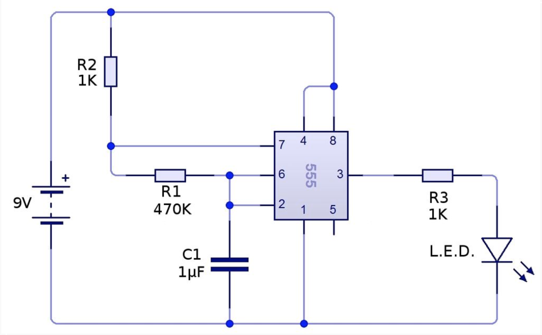
The LED 555 Timer Circuit
We will be building the circuit diagram of figure 1. This circuit creates a blinker by alternately charging and discharging the capacitor \(C_1\) in a continuous cycle.
Circuit Operation
The operation of this circuit can be understood in two distinct phases:
Charging Phase (LED ON)
- The capacitor \(C_1\) charges through resistors \(R_1\) and \(R_2\) with time constant \(\tau_{charge} = (R_1 + R_2) C_1\)
- The capacitor voltage is applied to both pins
2(TRIG) and6(THRES) - When \(v_{C_1}\) reaches \(\frac{2}{3}V_{CC}\) (the upper threshold), the comparator connected to pin
6triggers - This sets the SR flip-flop, causing the output (pin
3) to go HIGH - The HIGH output drives current through the LED and current-limiting resistor \(R_3\), turning the LED ON
Discharging Phase (LED OFF)
- When the flip-flop is set, the discharge transistor (connected to pin
7) turns ON - This connects pin
7directly to ground, providing a discharge path for \(C_1\) - The capacitor now discharges through \(R_1\) only, with time constant \(\tau_{discharge} = R_1 C_1\)
- When \(v_{C_1}\) falls to \(\frac{1}{3}V_{CC}\) (the lower threshold), the comparator connected to pin
2triggers - This resets the SR flip-flop, causing the output to go LOW
- The LOW output turns the LED OFF, and the cycle repeats
Timing Analysis
The timing periods can be calculated as:
- HIGH time (LED on): \(t_{high} = 0.693(R_1 + R_2)C_1\)
- LOW time (LED off): \(t_{low} = 0.693 R_1 C_1\)
- Total period: \(T = t_{high} + t_{low} = 0.693(2R_1 + R_2)C_1\)
- Frequency: \(f = \frac{1}{T} = \frac{1.44}{(2R_1 + R_2)C_1}\)
The duty cycle (percentage of time LED is on) is: \[\text{Duty cycle} = \frac{t_{high}}{T} = \frac{R_1 + R_2}{2R_1 + R_2}\]
Note that with this configuration, the duty cycle is always greater than 50% because \(R_2\) contributes to the charging time but not to the discharging time.
Bibliography
- Trilesto. "Flashing LED using 555 timer".